Research Interests
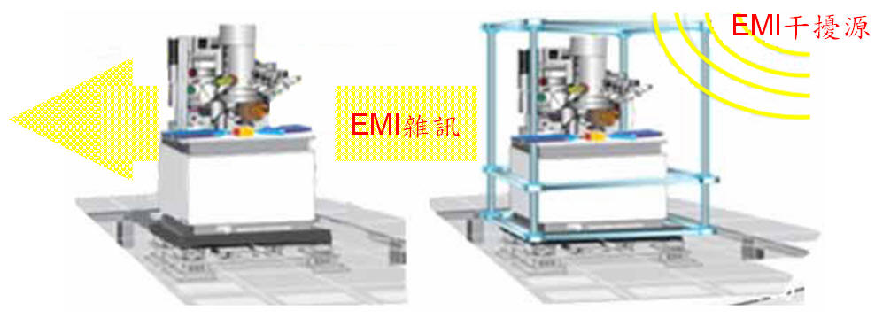
- Electromagnetic compatibility (EMC) includes electromagnetic interference (EMI) and electromagnetic susceptibility (EMS). EMI means that in the process of operation, the machine itself does not cause electromagnetic interference to other equipment. EMS means that even if the machine is subjected to electromagnetic interference from other equipment in the operation process, it still maintains its function.
The manufacturing of semiconductor industry in Taiwan is getting into 5nm linewidth below. It found that the extreme low frequency (ELF) magnetic field has negative impact on inspection equipment in manufacturing process, the precision equipment such as SEMs, TEMs, STEMs, FIB writers and E-beam writers are strongly demanded to operate in the environment which is below 0.5 m Gauss magnetic field intensity.
In general, there are two methods for reducing external magnetic interference: the active degaussing technique and the passive degaussing technique. Active degaussing technique uses a magnetic field sensor to induct the magnetic field and to demagnetize it with inverted magnetic field. Passive degaussing technique uses magnetic permeable materials or magnetic loss materials to isolate the external magnetic field. The advantages and disadvantages of these two technologies are described as follows:- The advantages of active degaussing technique are particularly effective in ELF electromagnetic interference. However, its disadvantage is that it can only be aimed at special frequency bands, and it will generate EMI, which interferes with other machines.
- The advantage of passive degaussing technique is that it can perform real-time degaussing in the frequency range above medium and high one. Nevertheless, its disadvantage is that the cost of the materials is expensive, and the improvement of the extreme-low frequency degaussing effect is limited.
電磁相容性Electromagnetic Compatibility (EMC)包括電磁干擾Electromagnetic Interference (EMI)及電磁耐受性Electromagnetic Susceptibility(EMS)兩部份。EMI是指機器本身在運作的過程中,不對其他設備產生電磁干擾;而EMS是指機器在運作的過程中,即使受到其他設備的電磁干擾,仍保持原有的性能。
臺灣半導體產業已經進入5奈米線寬以下,但發現極低頻(Extreme Low Frequency, ELF)磁場對製程檢驗設備之影響越來越嚴重,如電子顯微鏡SEMs、TEMs、STEMs、FIB writers、E-beam writers等相關精密儀器,強烈地被要求須在磁場強度低於 0.5毫高斯的環境下運作。一般而言,降低外部機台EMI的干擾方法有主動消磁技術與被動消磁技術兩種。主動消磁技術是利用磁場感測器進行磁場感應,並施與反相磁場進行消磁。被動消磁技術是利用導磁或磁損材料,用來隔絕外界的磁場,以下分別敘述兩個技術的優缺點:- 主動消磁技術的優點是針對極低頻電磁干擾特別有效,而缺點是只能針對特殊頻段進行消磁,且主動消磁技術會產生EMI,進而干擾其他機台。
- 被動消磁技術的優點是針對中高頻以上的頻段範圍,能進行即時的消磁,而缺點是材料價格昂貴,與極低頻消磁效果改善有限。
- There are three types of cleanrooms.
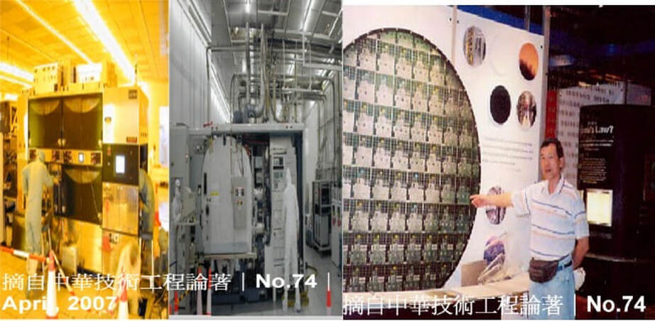
The 1st type is commonly used in industries where dust particle is a major problem, and their presence may prevent a product functioning as planned or reduce its useful life. For instance,manufacturers of microchip manufacturers are the major users of this type of cleanroom. This type can be called engineering or semiconductor cleanroom.
The 2nd type is applied to the industries such as biotechnology, pharmacy, medical devices, and food and drink, which require the absence of microbial, as their growth may contaminate in a product or infect a hospital patient. Usually, this type of cleanroom is named bio-cleanroom or pharmacy-cleanroom.
The 3rd type of cleanroom is built for dealing with toxic, pathogenic materials, and genetically modified organisms. If they can not be contained properly,it could cause hazard to human, environment and ecologic systems. The 3rd type is nicknamed as biosafety cleanroom or containment cleanroom.無塵室有三大類
第一類通常適用於,產業關鍵技術在防止灰塵及微顆粒污染的產業,其存在可能妨礙產品生產製造或減少產品之使用壽命。 例如,無塵室的主要用戶晶片製造商的製造商,此類型稱為工程或半導體無塵室。
第二類適用於生物技術、製藥、醫療設備、食品飲料等需要不含微生物的產業,因為它們的生長可能會污染產品或感染醫院病人。 通常,這種類型的無塵室稱為生物無塵室或藥房無塵室。
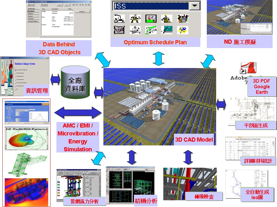
第三類無塵室適用於處理有毒、致病物質和轉基因生物。 其如果不能得到適當的控制,可能會對人類,環境和生態系統造成危害。 第三類又稱為生物無塵室或隔離無塵室。 - Generating and maintaining construction schedules from architectural drawings is vital to design and construction professionals for constructability review and project planning. Automating these tasks requires combining a CAD system with knowledge-based programming and data base techniques. A prototype system—called N-Dimension Project Management(ND-PM)—is presented for intelligent design, scheduling and construction.建築圖紙生成和維護施工進度表對於可施工性審查和項目規劃的設計和施工專業人員至關重要。 自動執行這些任務需要將CAD系統與基礎知識的編程和數據庫技術相互結合。而ND-PM的原型系統可展示智能設計、排程調度和施工模擬等等。
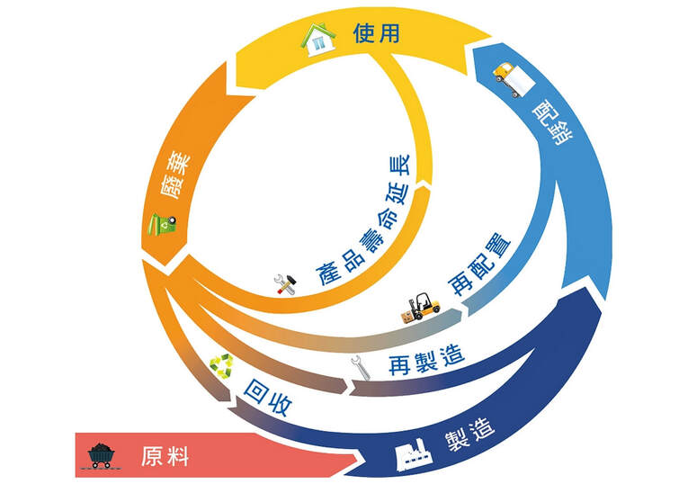
- Because of the extremely controlled environment, high-tech manufacturing plant/fab consumes a lot of energy and generates pollutants that harm humans and ecosystems. How to optimize the energy consumption and how to minimize the harmful pollutants will be critical subjects for future architects and engineers as well as manufacturers and the related suppliers. Many reports have indicated that intelligent and energy saving plant, , reduction of carbon dioxide, using renewable energy, solvent-free chemistry, catalysis and biocatalysis, life-cycle analysis, resource recovery, and recycling with smart plant design will form the corner stone in green facility/fab in near future.由於環境的精密控制要求,高科技廠房實驗室會消耗大量的能源,同時也會產生對人類和生態系統造成傷害的污染。如何能夠最有效的使用能源,以及如何降低污染物的傷害,將是未來研究之主要課題。許多研究指出,包含水電空調所需之能源節省,二氧化碳之降低,使用再生能源、無溶劑性化學藥品、催化劑及生物催化酵素,及其生命週期分析、資源回收再利用等等的智慧型廠房設計,是將來建造綠廠房設施技術的重要基石。
圖片來源:Innovate UK, Collaborations for a Circular Economy
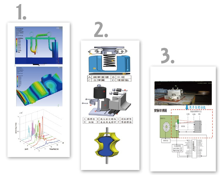
- As NT research advances, the increasing miniaturization of such items as microchips, processors, and devices demands the use of high performance microscopes (HPM,) and other precise instruments. To employ these microscopes and instruments, the processes involved often require a stable platform with acceptable level of vibration.
As the processes conducted in high-tech R&D&M, the vibration may be induced by earthquake, airflow, sound, traffic, near-by walking and door closing, electromagnetic interference (EMI), radio frequency (RF), or light quantum effect. When facilities grow more complex and miniaturized, vibration has become increasingly more important than the years when the demand for higher precision tools grows. (Bayat and Gordon 1998)
As far as the microelectronics industry is concerned, whereby microprocessors and semiconductor technology is produced, many tools are very sensitive to vibration. Meanwhile, sound wave becomes a growing concern since noise and floor vibration particularly affects in-process experimentation and nano-fabrication. For example, processes involving electron beams or probes, where the goal is to develop precise images of the surface, require a stable environment for relative positioning of the beam or probe, as well as for the object being scanned. Otherwise, the scanned image may appear to be in various locations at once and may be overlooked. “Both vibration and excessive thermal variation can interfere with the stability of these processes.” (Amick et al. 2002)奈米科技的研發製造,微晶片、微處理器和精密儀器設備等等的微型化精密度要求逐漸提高,極須使用高性能顯微鏡(HPM)以及其他高精確度儀器。為了善用此類顯微鏡和儀器,其使用過程通常需要一個可接受震動水準的穩定平台。
因為在高科技的研究、發展與製造過程中,震動可能源於地震、氣流、噪音、交通、關門、電磁波干擾(EMI)、射頻(RF)或其他光量子波動效應。在製造設備更為複雜且更要求微型化更精密時,震動影響之重要性在奈米科技之發展時程上已逐漸超越過去對製造設備精密度的要求(Bayat and Gordon 1998)。
就微電子技術工業而言,微處理器和半導體科技的生產過程,很多工具對振動是非常敏感的。同時,因為噪音和地板振動格外影響進行中的實驗和奈米製造過程,故聲波成為日益關心的議題。例如,利用電子束或電子探查發展物體表面精確影像過程,需要穩定的環境以利電子束或探針以及被掃描物體的定位。否則,被掃描的圖像可能模糊不清同時出現在不同的位置並且可能被錯誤判讀。振動和過度的溫度變化二者皆能干擾這些過程的穩定。(Amick et al.2002.)- 調查與分析廠房設施振動傳遞狀況
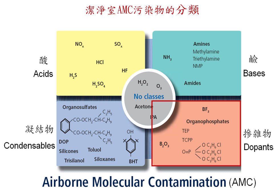
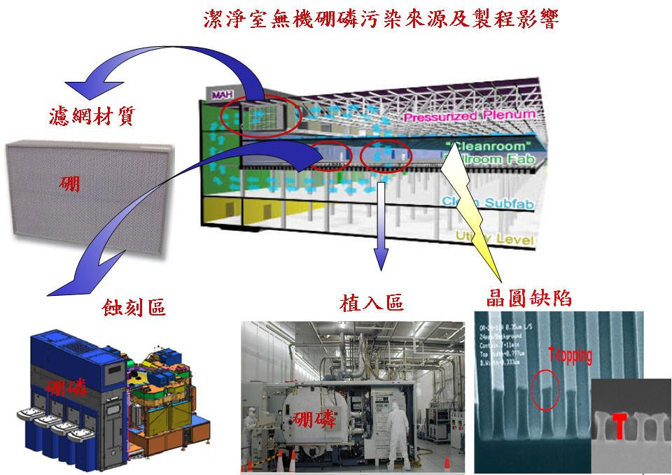
- 選擇隔振參數與合適的隔振系統
- 如有不足,加上單軸減振器降低單一機器主要振動頻率之振幅,其次組合單軸減振系統或採用多軸減振系統,降低 多設施組合振動或單設施多模態振動,最後考慮浮動減振 平台。
- This research is to detect boron phosphorous air molecular contamination in clean room. Present method is not effective. The researcher must spend 24 hours or more to collect boron and phosphorous contamination in clean room. This severely inhibits efficient production process. There is a need to shorten the duration to timely detect the boron and phosphorous contamination within a few hours. 旨在檢測無塵室中的空氣污染分子-硼磷,目前的檢測方式效益不大,研究人員必須花24小時或更長時間在無塵室中收集硼和磷的污染物,嚴重影響生產效率,需有效改善檢測時間,並縮短在幾小時內可及時檢測硼、磷之污染。
